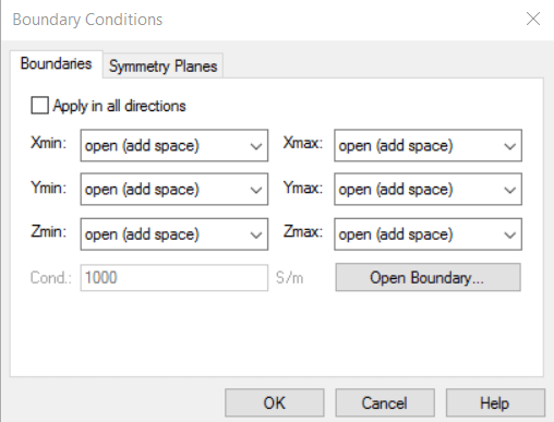
The simulation of long transmission lines in CST can get very messy sometimes, exhibit discontinuities and ripples in the s-parameters plots. This is usually the result of unwanted reflections due to improper boundary conditions. In such cases, the solution to the problem is to modify the boundary conditions of the simulation: Instead of having open boundary conditions with open space for the side walls and the bottom of the substrate, it is more appropriate to have just open boundary conditions (without open space).
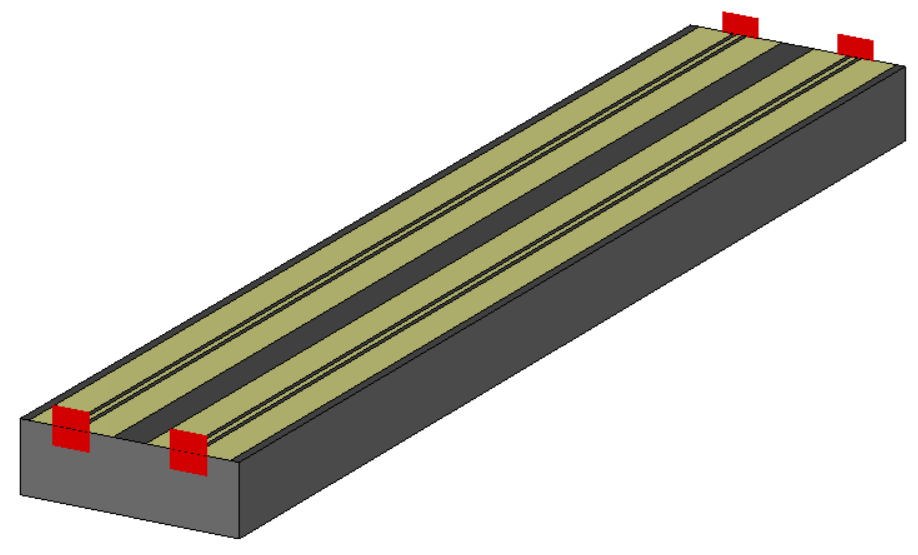
Here is an example of two CPW lines in a 600-μm thick silicon substrate (εr =11.66) and a total length of 10 mm. The width of center conductor was set to 50 μm and the gap between the lines was set to 35 μm, as shown in the figure below. Since the there are two CPW lines, there are a total of four ports.
When the simulations are performed using the frequency domain solver (the most appropriate choice for transmission lines and waveguides) with the following boundary conditions settings:
One obtains the following results:
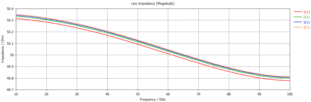
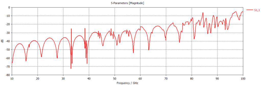
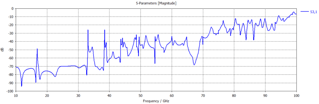
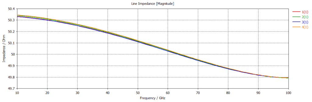
Although the result for the line impedance is correct and shows no numerical artifacts. The results for S11 and S31, i.e. the reflection coefficient and the crosstalk coefficient show a lot of numeral artifacts which are difficult to ignore or remove. They are most likely caused by the long length of structure, which effectively behaves as a high Q resonator.
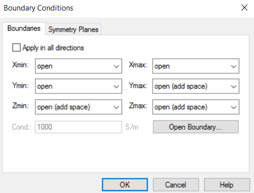
By changing the boundary conditions on the lateral walls and on the bottom of the substrate to open (without space), the simulator can treat those boundaries as absorbers, effectively reducing the Q of the structure. Thus, when switches to the following boundary conditions:
The obtained results are:
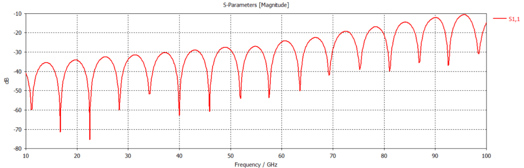
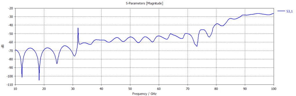
As it is evident, the results improved significantly.

Leave a comment